How did I get into this mess?
One of my housemates came into posession of a Pikachu N64.
A slight issue - it's NTSC, and we only had PAL games.
At first I tried replacing the CIC in one of the games with an UltraCIC which reimplements the CIC protocol on an ATTiny (see here), but this lead to it generating a NTSC video signal at 50Hz, as the game controls how fast the refresh rate is. None of the displays/capture devices I had managed to handle this, so it's back to the drawing board.
I figured the N64 bus is relatively low speed, and decided to make it A Project™.
Hardware
I opted for a 512Mbit SDRAM to hold cartridge data as that's the largest possible N64 game, and an iCE40 HX4K FPGA to handle the cartridge bus, as it's supposed by the open source [IceStorm] tools.
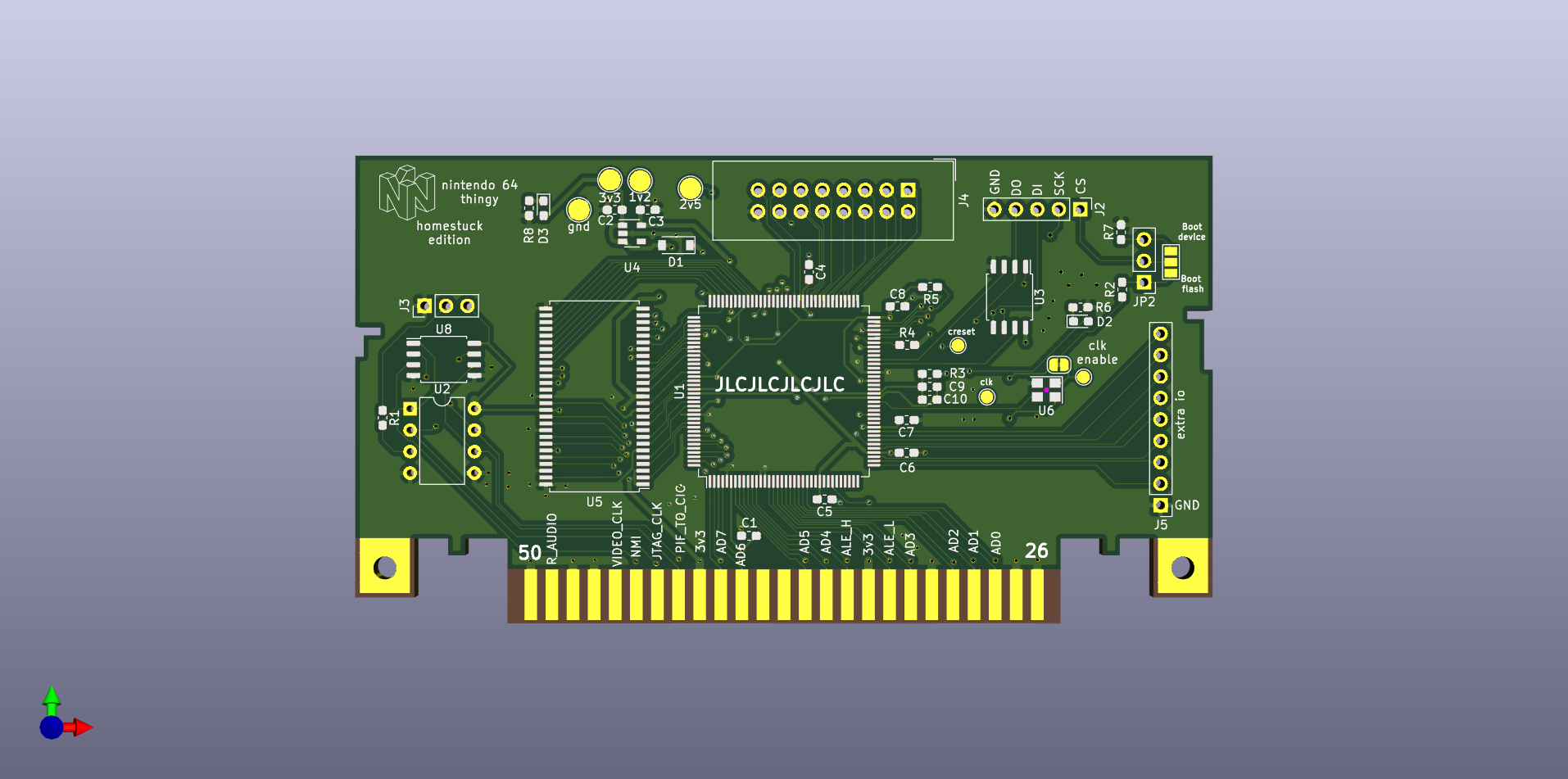
This mirror of an old page is the only real resource I managed to find on the N64 bus timings, but has been extremely valuable.
The cartridge bus is 16 bits wide, with the address multiplexed onto it - the address gets latched by ALE_L/ALE_H. !READ/!WRITE indicate a read/write on the bus, automatically incrementing the address.
Gateware
At first, I added support for my board to the LiteX SoC framework, as a way to test that the hardware was okay. In the long run I want to develop a custom SoC using the SERV RISC-V core and a simplified bus structure, as the LiteX SoC had things that aren't needed, like the ability to run code from DRAM. This makes it quite large...
Info: Device utilisation:
Info: 	         ICESTORM_LC:  6135/ 7680    79%
Info: 	        ICESTORM_RAM:    29/   32    90%
Info: 	               SB_IO:    51/  256    19%
Info: 	               SB_GB:     8/    8   100%
Info: 	        ICESTORM_PLL:     1/    2    50%
Info: 	         SB_WARMBOOT:     0/    1     0%
but it was good for testing.
--========== Initialization ============--
Initializing SDRAM...
SDRAM now under software control
SDRAM now under hardware control
Memtest OK
Memspeed Writes: 1Mbps Reads: 2Mbps
Gateware - attempt 2
For this I need a custom SDRAM controller - ideally it can be simplified by only supporting long burst data read/writes, as reading from SPI flash / SD card into SDRAM should be done in long bursts. The N64 protocol lends itself well to reading a 256 byte chunk from RAM whenever the address is set explictly, as there can be up to 256 bytes read between ALE_L pulses.
I've been trying to implement this, but it doesn't work on hardware (yet).
As something else to do I implemented the N64 bus protocol and logged the read addresses into a block ram - it's capable of reading the bootcode (also stored in block ram for now) and starting to read the rest of the ROM (for checksumming).
00 10000000 8037
01 10000002 1240
02 10000040 4080
03 10000042 6800
04 10000044 4080
05 10000046 4800
06 10000048 4080
[ ... reading the rest of the bootcode ... ]
f6 10100ff8 0000
f7 10100ffa 0000
f8 10100ffc 0000
f9 10100ffe 0000
fa 10000008 8024
fb 1000000a 6000
fc 10000010 635a
fd 10000012 2bff
[ etc, reading the first 1MB ]
-		m.d.comb += Cat(ram.we, ram.cas, ram.ras, ram.cs).eq(cmd)
+		m.d.comb += Cat(ram.we, ram.cas, ram.ras, ram.cs).eq(~cmd)
now it (mostly) works
ugh
this took me far too long to figure out
Now that I have a SDRAM controller (mostly) working, I decided to get a CPU core executing some code. This turned out to be harder than I thought..
A few issues I ran into along the way:
- SERV isn't very resilient against misbehaving Wishbone devices
This meant that when my Wishbone RAM module was holding ack high past when SERV dropped cyc, some extra logic was being enabled that made everything fail in weird ways.
Thanks to Olof for helping me figure this out!
- my RAM was full of other bugs
Some issues: I accidentally left the write port enable activated after a write finished, which meant that reads were broken. This looked like it was some kind of simulation/timing bug, due to Yosys write transparency logic forwarding the written data to the read port.
Another more subtle case of this is that I left the write port enable active for one cycle after cyc was deasserted - SERV drops the value on the data bus as it drops cyc, meaning some garbage was written to the memory instead.
So now I have some assembly and some C code running and (mostly) working. Next up is probably a core that can take data from SPI flash and transfer it into RAM as quickly as possible. After that all I need is to hook up the N64 side to RAM reads and things should mostly work.
Of course for this to be possible I need to fix the SDRAM controller first...
This is a diagram I've had lying around on some paper for a while, I got around to adding a couple edges to it + rewriting it in Dia.
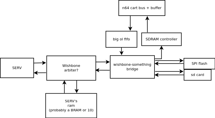
There aren't a lot of peripherals that are actually needed for a first test - just SPI flash & SDRAM.
So far I've updated everything to the latest versions (nMigen -> Amaranth) and updated the external cores (CPU, SPI flash controller). I found a few more bugs in things I thought were good, like my RAM block working entirely by accident - PicoRV32 which I was testing with before only sets sel when writing, but SERV sets it to garbage values when processing things. My RAM had a statement wr.en.eq(Mux(passthrough_wr, 0, self.bus.sel)) to pass the sel signal through to the RAM when passthrough_wr is set, but that instead passes it through when not set.
Also, I've looked at using LiteDRAM again - I had some issues with my DRAM controller on hardware I couldn't quite shake out, so I want to use something I know that works.
Here's the new block diagram:
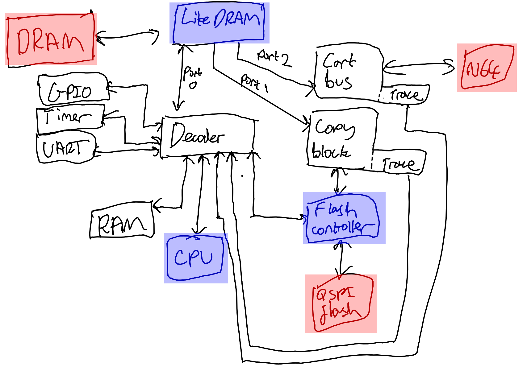 All of these bus connections are Wishbone. Here, hardware components are marked with a red tint, and external logic IPs are marked with a blue tint.
I've been able to validate that data is read out of the SPI flash and into the DRAM sucessfully, by reading it out of the CPU-connected port.
There's still some lingering issues in the cartridge block, where I think sometimes it's missing pulses on !READ. This is sort of expected as the activity we're looking at is a 60ns pulse, regardless of any of the other timings...